Creating tiny, detailed patterns on silicon wafers is key to building powerful chips. However, when designs get complex, standard methods don’t always work. That’s where silicon wafer patterning solutions made just for your needs can help.
These custom solutions use advanced tools to create sharp, accurate patterns even for the most detailed layouts. Whether you’re building cutting-edge tech or unique microchips, tailored patterning offers the precision and flexibility you need to succeed in today’s fast-changing semiconductor world.
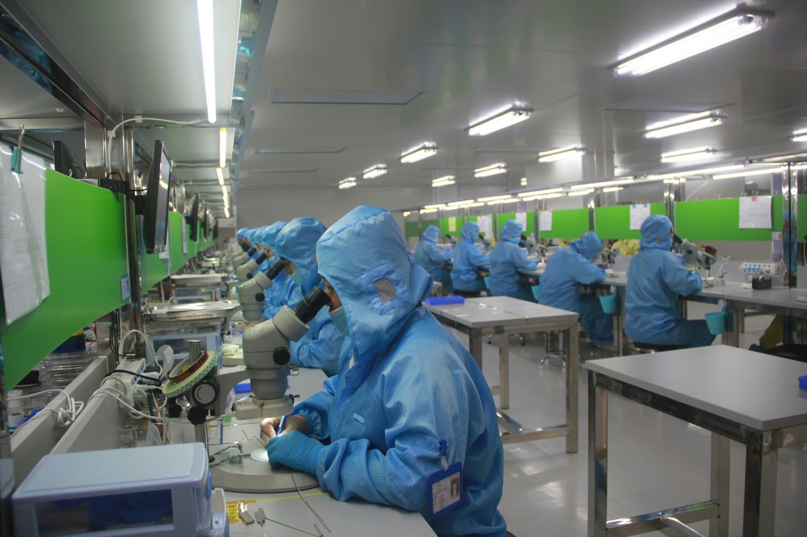
Understanding Silicon Wafer Patterning
Silicon wafer patterning is the process of creating tiny circuits and features on a silicon surface. It involves using light or chemicals to form patterns that guide how the chip works. This step is critical in making modern electronics fast and reliable.
Each pattern must be clean and exact. Even the smallest mistake can affect the whole chip’s performance. That’s why experts use special tools and methods to make sure each pattern is perfect.
Tailored solutions go beyond standard processes. They are made to match specific needs and designs. This level of control allows for better results in high-demand applications.
The Importance of Customization
Every chip has a unique purpose. Because of this, the design and pattern on the wafer must match that purpose exactly. Customization ensures the chip performs as expected.
With custom wafer patterning, engineers can create layouts that fit complex functions. This is especially useful in medical devices, defense systems, and AI tools. Tailored designs save time and reduce errors during production.
Customization also means better use of materials. It prevents waste and improves the efficiency of the entire process. This leads to higher-quality chips at a lower cost.
Challenges with Complex Designs
As chips become smaller and more powerful, their designs also get more complex. These new layouts are harder to produce using standard tools. Small errors can ruin an entire wafer.
That’s why companies need more advanced patterning solutions. These solutions are made to handle tight spaces, tiny features, and detailed shapes. They reduce risks and help meet modern design demands.
Engineers must also work faster than ever. Tailored solutions allow for quicker changes and updates without losing accuracy. This keeps production on track even with the most complicated layouts.
Advanced Lithography Techniques
One key part of wafer patterning is lithography. This is where light is used to draw the pattern on the wafer. Over time, these tools have become more powerful and precise.
Advanced lithography techniques include deep ultraviolet (DUV) and extreme ultraviolet (EUV) methods. These allow for ultra-small features with high accuracy. They help meet the needs of today’s top-tier chip designs.
These tools also support layering, which is crucial for 3D chip designs. More layers mean more power in a smaller space. Tailored lithography supports this growth by providing the needed flexibility.
Precision Wafer Etching for Better Detail
Etching is the next step after patterning. It removes unwanted parts of the silicon to shape the circuit. This step must be very accurate.
Precision wafer etching uses advanced chemicals or plasma to make fine cuts. This keeps the features clean and sharp. It is important for building small and detailed components.
Tailored etching solutions allow engineers to control the depth and shape of every cut. This means better performance and fewer errors. It’s a must for complex microchip designs.
Photomask Customization and Accuracy
A photomask is like a stencil used in lithography. It carries the pattern that will be printed on the wafer. A clear and accurate mask is key to quality chips.
With photomask customization, each design gets its own mask. This ensures high accuracy and repeatability. Custom masks help avoid problems during mass production.
These masks are made using lasers and special materials. Tailored tools check them for flaws before use. This keeps the whole process reliable and consistent.
Solutions for Complex Microchip Layouts
Chips used in Artificial Intelligence (AI), 5G, and space tech often have complex layouts. These layouts are dense and full of tiny details. Standard patterning cannot handle these designs well.
Complex microchip layouts need advanced planning and tools. Tailored solutions offer both. They ensure every line and feature is placed with care.
These solutions are also flexible. They adapt to changes and design upgrades quickly. This is important in fast-moving industries.
Streamlining Silicon Wafer Processing
Wafer patterning is just one step in a long process. Other steps include doping, polishing, and layering. All these must work together smoothly.
Silicon wafer processing solutions bring all steps into one flow. They reduce delays and improve output. This helps companies meet production goals.
Tailored systems match each stage with the chip’s needs. This saves time and money. It also improves the overall quality of the final product.
Using Semiconductor Design Services
Sometimes, companies need outside help for complex projects. Semiconductor design services offer expert support. These services bring experience, tools, and advice.
Design firms help with layout planning and tool selection. They work closely with engineers to create the best patterning plan. Their input often improves yield and lowers costs.
They also test the final design before production. This step is important for catching mistakes early. It adds value and confidence to the process.
Benefits of Patterned Silicon Wafers
Using patterned silicon wafers saves time during chip manufacturing. The wafers already have the needed patterns, so fewer steps are required. This makes production faster and more cost-effective.
Patterned wafers are also more reliable. The patterns are made under controlled settings, reducing the chance of errors. This helps improve the yield in final chip production.
They are ideal for research and small-batch work too. Scientists can test ideas without making a full production run. This is helpful for innovation and rapid testing.
Advancing Technology with Silicon Wafer Patterning Solutions
Silicon wafer patterning solutions help create detailed and accurate chip designs. They offer better control, speed, and quality for complex projects. These solutions are key in meeting the growing demands of modern technology.
With the right tools and custom methods, engineers can build stronger and smaller chips. This leads to better products in less time. Tailored solutions also help reduce waste and lower costs. As designs get more advanced, silicon wafer patterning solutions will stay important for future success.
Did you find this article helpful? Visit more of our blogs.